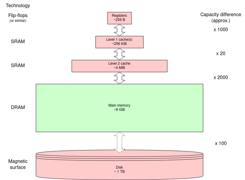
DRAM has been the technology of choice for its capacity for many decades. This is because the size of each bit store is much smaller than other (semiconductor) storage so more bits can be fitted in a given chip area.
Here, we only care about the externally properties of the memory. If you want to know more about the internal engineering, there is a nice video from Microchip Technology. (This was also on the previous page.)
What is DRAM? (7 mins.) (2018)
However, the internal structure does affect both the way the memory is accessed and, critically, its timing properties.
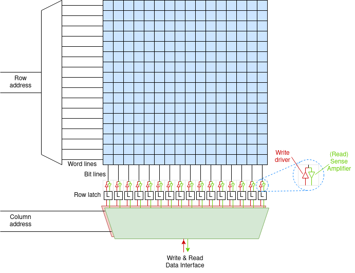
The memory is implemented on silicon as a 2D matrix: a
two-dimensional array. It is like the figure below except there will
be many more rows and columns: a few ‘k’ in each dimension
and always a power of two. The bit cells as drawn are built to
tessellate with ‘word lines’ carrying the row address to
the matrix and ‘bit lines’ carrying data to/from the
cells. This minimises the wiring which means the cells can be as
small as possible.
Each cell (as drawn here) may contain one or more bit cells; each
column of bit cells has its own bit line.
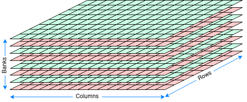
Bigger means slower and making the matrix too big will slow it down. Thus a modern DRAM chip will typically contain several (say eight) such matrices or banks. These also have some independent address bits. This makes the logical view of the chip three dimensional (although the banks are really side by side on the 2D silicon surface.
The structure of the DRAM dictates the access process. For a read (writes are similar):
This means parts of the address are sent at different times so the appropriate address bits can share the same wires. E.g. 12 address bits can allow access to a bank of up to 16 Mi (224) elements. The meaning of the address argument is specified by a command.
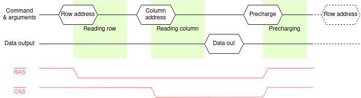
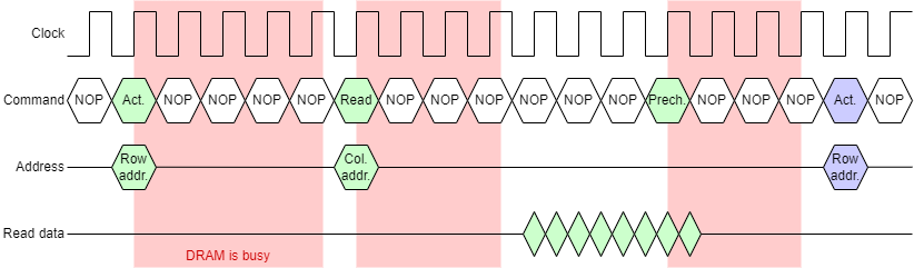
The timing diagram shows an example read cycle. The pale red traces show two signals from a now largely superseded interface although the names still crop up in descriptions so they are included here. Modern interfaces will be described under ‘SDRAM’. The historical signals are (active low) Row Address Strobe and Column Address Strobe and these changing indicated the timing. Following the command - and this is still relevant - there is a time when the DRAM is busy operating internally. These times are shaded green in the figure; they are fixed times for a given DRAM device.
These internal delays dictate the minimum latency of the DRAM operations. The DRAM can go slower than these (all different) times but not faster. In general (and certainly in the case of SDRAM) the commands are sent from a clocked system so there is typically some ‘slack’ time.
Although there is not much point, the DRAM could go quite a lot slower. However there is a maximum time time too because of the need for refresh.
Internally there is a capacitor and it leaks any charge away over time. Ignoring the engineering detail, there is a limited time which any cell will stay valid. In any case, any access to a cell will destroy the contents of every cell in the selected row. However the row's data are captured and restored (in full) during the precharge part of the cycle.
Thus, if the memory is in regular use, these actions
will refresh the used rows. To guarantee all rows are
refreshed it is usual to run refresh cycles in the background, cycling
through all the rows in the bank.
Note that some banks can be refreshed in parallel with others being
used and several banks can be refreshed in parallel.
The refresh mechanism has to service every row in a period of the order of tens of milliseconds - i.e. a few dozen cycles per second - so it is not too intrusive. A refresh operation can be faster than a read operation since it does not need the ‘column’ part of the cycle, just an activate and precharge.
Modern SDRAMs typically have a self-refresh mode so that they don't need a command for each row. This is useful if, for example, the processor is ‘sleeping’. There is some added latency because this may need to be turned off when waking up.
DRAM is Dynamic Random Access Memory. The “Dynamic” part refers to the fact that it is not all that great at remembering - so it needs a continual refresh process to reinforce its contents.
Here's a video which is (sort-of!) an analogy. :-)
The “Random” part refers to the ‘fact’ that any address can be read (or written) at any time with the same access time. This is not quite true with DRAM; however it is a lot more ‘random’ than technology such as magnetic tape which indicated ‘computer’ in old science fiction movies. (There's a much longer (15 min.) guide to these tape drives, here.)
The figure below represents a small DRAM holding 128 4-bit values: 8 rows each with 16 columns. A ‘real’ DRAM bank will be larger in all dimensions - always a power of 2 to make address mapping easy.
The (scale) figure below shows some possible ways or mapping DRAM chips into a 64-bit address space. These are sensible alternatives, but certainly not the only possibilities.
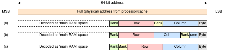
In each case the most significant bits are used to determine where, in the physical address space, the main memory is. In practice not all of these may be considered when decoding, in which case the memory will be aliased and appear repeated in several places.
What's a ‘rank’? A rank is (roughly) a DRAM module. When you add memory to your machine you will be adding ranks. Ranks are addressed by high-order bits so that whatever memory is present will appear contiguous.
The least significant bits choose the byte within the word. In most cases these will not be used here since all transactions will be word length or greater. In the example above a 64-bit memory word is assumed but a longer ‘word’ between the DRAM and the cache gives higher transfer bandwidth (at the price of more wires).
In the alternatives shown (at least some of) the column address
bits are the least significant used bits. This ensures that a burst
to/from the DRAM provides contiguous words which map to a cache
line,
The alternatives shown map the spaces as follows:
(a) The columns are interleaved such that successive addresses map along a row but move to the same row in another bank until each bank has been addressed.
(b) The interleaving is at cache line granularity so that successive cache line fetches will come from different banks.
(c) The banks are not interleaved so successive addresses will go completely through the banks one at a time.
Different mappings may yield different performance, for example by being able to request multiple transfers from a row whilst it is still ‘open’ (i.e. ‘activated’). This can depend on what is doing the requests; for example a GPU probably uses longer and more predictable transfers than a processor cache line fetch.
The DRAM controller turns the user's address into a command sequence for the DRAM chips. After performing (say) a read operation it can precharge (write back) the row or leave it ‘open’. The first of these ‘policies’ prepares the DRAM for the next ‘random’ read; the second will be slower (it must precharge before starting) unless the next request is to the same row - in which case it will be considerably faster. Optimisation depends on predicting the future.
A ‘smart’ controller might vary its policy heuristically although the ‘best’ approach seems still to be a matter of debate.
Problem: note down what you think might be the advantages and disadvantages of a controller using each of the above strategies. Consider the effects on speed, power etc.
Does the ‘best’ strategy vary according to the task being done?
Do you have any suggestions for a ‘perfect’ system?
Firstly, SDRAM is Synchronous Dynamic Random Access Memory; it is a form of DRAM and not related to SRAM. The Synchronous operation is because the RAM chips contain a state machine which runs from a supplied clock. This relieves the load on the memory controller but the internal operations are the same as earlier DRAM devices.
The sequencing of the SDRAM interface justifies its own controller. The controller intermediates between the processor(s) - or, more likely, the cache controllers - and the SDRAM chips. This will usually make the interface look quite straightforward from the outside although there will be some uncertainties in the exact timing.
It is anticipated that the SDRAMs will be ‘below’ a cache (or similar) memory. Code and data caches tend to assume things about locality so transfer whole cache lines rather than single bytes or words. To support this SDRAMs usually operate with (programmable) data bursts rather than single transfers. Once a column access has started an internal address counter multiplexes successive addresses. This can be very rapid which improves the overall transfer bandwidth.
The SDRAM's internal timings must be accommodated by the clock. It
is the (system) programmer's responsibility to know the clock period
being used by the controller - and fed to the SDRAM(s) - and provide
enough clock periods to meet the timing requirements.
For example, the SDRAMs may be told ‘send the read data bursts
starting from four clocks after the read command’. The returned data
can then be ‘captured’ at that time.
This example is a DDR SDRAM; as drawn the clock rate appears to have been optimised to maximise the transfer rate: i.e. the data values just stabilise before changing again.
Note: the figure is somewhat simplified for clarity. In the real engineering of the interface the return data is synchronised with the clock as delayed by being passed across the PCB to the SDRAM module and delayed again on the return trip.
This affects the latency but doesn't spoil the principle, so let's ignore it here!
To perform a typical read operation the controller will need to perform the following operations:
This demonstration is animated to illustrate the timing characteristics. Note the pauses between commands whilst the SDRAM chip works internally. This gives SDRAM a long latency. However the data transfer bursts give high transfer bandwidth.
The data burst will typically be set up to fill (or empty) a cache line [link]. Originally a data word would be passed on each consecutive clock cycle; modern devices are usually a DDR (Double Data Rate) variant which supplies two words in each clock cycle (one each on the rising and falling clock edges). This gives the SDRAM a (potentially) high bandwidth.
Burst size will usually be programmable at set-up time. If some
data is not wanted it can simply be ignored. Write operations are
typically also bursts; in this case an enable signal
accompanies each element so that only the desired elements are
changed. (In the demonstration only the non-blank entries are
written.
Bursts will normally be address aligned. For example with
bursts of four elements the addresses will be multiples of four. This
fits ‘naturally’ with a cache controller etc. The alignment can
sometimes be abused although the burst will (on most SDRAMs) wrap
around the end of a row.
The inside of the SDRAM chip(s) will be divided into banks. These are, effectively, independent DRAM devices. This allows concurrent operations within the chip. For example, after a row activation has been sent to one bank there will be a pause whilst the command is obeyed. It may be possible to send an independent command to another bank in the interim, thus interleaving different operations and achieving better utilisation. This relies on having multiple independent operations to perform: perhaps unlikely with a single processor but useful when the SDRAM is shared amongst multiple cores [link], GPUs etc.
As a guide, a single SDRAM might have eight independent banks.
The SDRAM controller will also keep track of time and insert refresh cycles as needed between the user's commands.
Supplementary material
Clear, if slightly dated, slide set covering SDRAM and SDRAM controllers in a bit more detail.
Next: Error detection & correction