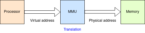
A Memory Management Unit (MMU) is not vital for a computer but is used to support the operation of virtual memory. Its chief function is address translation, with other functions such as memory protection.
Logically this is simply a pattern translation. However various expedients are needed to be able to implement the process practically. The translation process is implicitly serial in the memory access and therefore can increase the latency of every access. This would be a serious penalty.
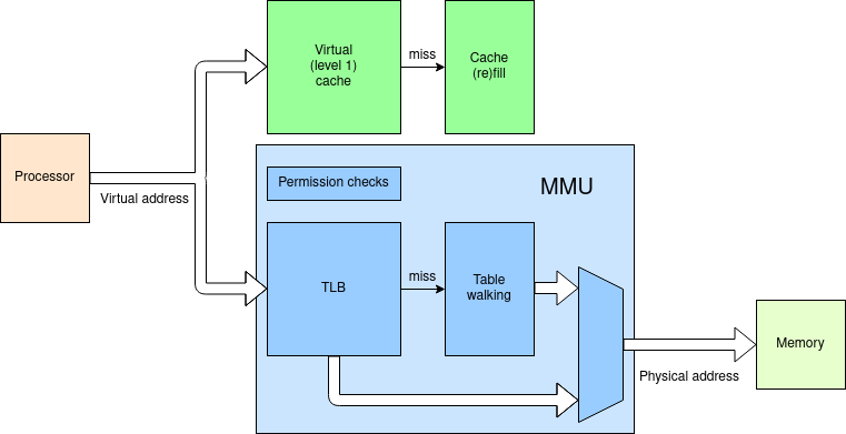
The usual approach is to provide a virtually addressed cache to avoid
the translation delay ... as long as that cache hits. This first
level of cache needs to be fast: it is therefore quite small.
In parallel with the level 1 cache look up, the MMU can
provide an address translation in case the cache misses.
Translation is provided via page tables. The page tables can be large: they are stored in memory. Thus each translation is subject to the latency of the main memory. Worse – with 32- and 64-bit address spaces it is impractical to store fully expanded page tables for every possible process, so the page tables are divided into multiple ‘levels’: perhaps two levels in a 32-bit system, more in a 64-bit address space. This means that multiple memory look-ups are needed for each memory reference. Unalleviated, this would be cripplingly slow!
The Translation Lookaside Buffer (TLB) is a cache of address
translations. Using the same principle as memory caches, it holds
a subset of the possible page translations; statistically only a few
of the possible pages wanted by a process are in use and even fewer
needed at a particular moment, thus all or nearly all translations can
be looked up very rapidly.
Note that what is cached encompasses all the page table levels in one
operation: virtual address in to physical address out.
 (5 mins.) (2014)
If/when a TLB miss occurs the page tables must be read and references
followed. This will take some time – possibly hundreds of processor
cycles. The operation is provided by a hardware machine in a process
called "table walking". Whilst this proceeds the originating process
has to be suspended.
In a multi-threaded processor
it is possible to continue
running other threads (which share the same virtual memory map) in
parallel with table walking, keeping the processor busy.
Page tables are specific to each process. When context switching the MMU is reprogrammed with a pointer to the appropriate (first level) page table. Note that this invalidates the contents of the level 1 cache(s) and the TLB and they must be flushed, as appropriate. The TLB and instruction caches can typically be discarded: a data cache may contain modified (‘dirty’) locations and thus need a significant time to copy all the updated lines back down the memory hierarchy.
Small systems (typically embedded systems) may not afford the effort to implement a full MMU. In particular, a TLB can consume considerable silicon area. A Memory Protection Unit (MPU) provides permission checks for areas or memory without the virtual-to-physical translation.
A simple but important function of an MMU (or MPU) is to mark which
addresses can be cached and which cannot. In general, memory can be
cached and this will enable significant speed up. On the other hand,
areas of the address space used for I/O must not be cached since they
can (and will) change contents without processor actions. Similarly
memory which is involved in active DMA transfers should not be
cached.
A related issue is whether write operations area allowed to
be buffered
and this may be another
‘enable’ bit on each page/area.

In a computing system there is sometimes often a need for
some ‘bulk’ storage outside the programmer's direct view.
This is usually in the form of a buffer. Buffers are used
extensively to avoid strict synchronisation between components. For
example, data may be streamed from a network connection at the
network's rate into a RAM buffer and then read out – perhaps
by DMA
– at a different rate. Network routers, for example, often do
this to store-and-forward packets.
For most on-chip applications this will be implemented with blocks of SRAM.
A problem with using SRAM as a buffer is that the normal SRAM has
a single port – i.e. there can only be a single access
(read or write) at any time. This imposes a bandwidth
limit.
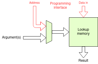
Another application for a RAM (almost always SRAM) – or, indeed a ROM – as a component might be a lookup table. Some functions (such as logarithms or trig. functions) can be quite expensive to calculate: a lookup is an array which contains precalculated answers and can supply arbitrary functions in a single memory cycle time.
Often associated with software, a lookup can also be used as part of a
hardware calculation system. The input argument(s) form the
‘address’ and the data is the data.
Lookups can be useful for monadic (one argument) functions –
less useful with two (or more) arguments since the address needs to be
the concatenation of the inputs so the size of the table
expands rapidly.
It is possible to engineer multiport memory arrays but there are some difficulties. For a dual-port RAM:
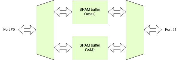
An alternative mechanism is to make a unit which is almost as good (probably better when the disadvantages above are averted) by interleaving locations in single-port RAM blocks. When one port is connected to one part of the buffer the other port can still use the other. As long as there are no conflicts the buffer system has twice the bandwidth of either block.
Deduction: in the figure the SRAM arrays have been labelled ‘even’ and ‘odd’. This is a hint! Which addresses (think address bits) would be routed to each block and why?
You need to consider how such a buffer is typically employed and what the address sequences might be to make sense of this.
It is, of course, possible to generalise this concept and use more
‘ways’ of interleaving. This further reduces the chance
of conflicts (but to a lesser extent than the first step of
interleaving). Assuming there is a minimum practical size to the
component arrays (which there is!), further interleaving does increase
the incremental size of the overall buffer.
E.g. if the SRAM comes in 1 KiB blocks a 2-way interleaved system
can be 2 KiB, 4 KiB etc. but a 4-way interleaved system can
only be 4 KiB, 8 KiB and so on. The area may be a
concern.
Next: Memory.