Introduction to SRAM
- Static
- Random
- Access
- Memory
SRAM technology
SRAM is probably the simplest memory technology in general use. It
is fairly simple to manufacture on the same chips used for processors,
logic etc. and is easy to use. It is used for various small memory
applications such as:
- Microcontrollers with small RAM requirements
- Dedicated ‘on-chip’ memories
- Caches and cache tags
- Routeing tables
- FPGA applications (as embedded ‘block RAMs’
- Temporary Buffers, such as in a network interface
- etc.
SRAM is quite dense (in terms of the number of bits stored
in a square millimetre of chip surface, though not nearly as dense as
the (less convenient) DRAM. It is quite fast, though not as fast as
registers made from flip-flops.
Here, we only care about the externally properties of the memory.
Feel free to skip this insert if not interested.
If you want to know more about the internal engineering, there is a
video from Microchip
Technology. (This was also on the previous page.)
 What is SRAM? (5 mins.) (2018)
A couple of things this video doesn't mention or emphasise are that:
What is SRAM? (5 mins.) (2018)
A couple of things this video doesn't mention or emphasise are that:
- To save space the transistors in each bit cell are as small
as possible; this makes them very ‘weak’ (electrically -
pardon the simplification) so they need extra time to drive the output
when read.
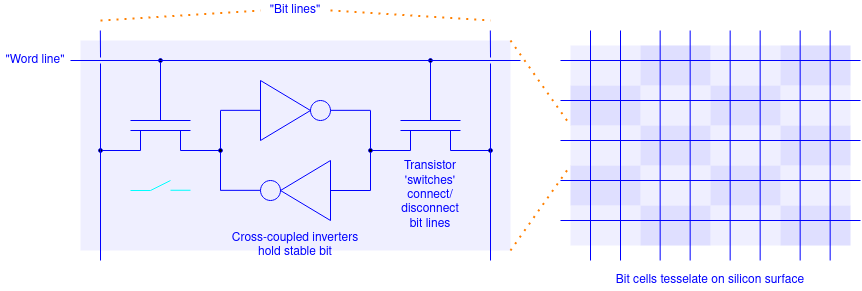
- To speed up operation, differential sense amplifiers are
used across the complementary bit lines to detect a small difference
as it develops and amplify this into a full logic level. These
amplifiers are quite power-hungry.
- As the SRAM bit array gets bigger the bit lines get longer (thus
higher capacitance) so the SRAM slows down.
[There's also a bit of an ‘oops!’ at around 1:30 😲
– can you spot the error? (There's a slip of the tongue near
the end, too.) Still a very good video.]
The important points are that:
Bigger (in a ‘number-of-bits’ sense means
slower.
Read and write times are the same and
constant, irrespective of the address. This is often arranged to be a
single clock cycle.
SRAM is volatile in the sense that it holds data only
whilst it remains powered.
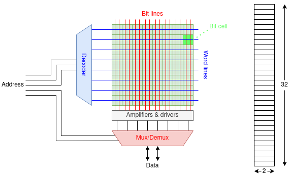
The memory is laid out on the silicon in a rectangle which
is fairly close to being square. This keeps it compact and
keeps the wire length ‘under control’. This contrasts
with the memory as pictured in software which is very
‘long’ and ‘thin’.
The adjacent figure shows the two views (of an artificially small
array) and how address bits are split in practice.
This is not visible from the outside
– so, maybe you don't care! However something
similar is used in DRAM and SDRAM where it does influence
behaviour.
SRAM in operation
Historically, SRAM was asynchronous, meaning it acted like
combinatorial logic. When reading you input an address and, some time
later, the data appeared.
Most modern SRAM is synchronous in that it has a
‘wrapper’ with a clock. Feed it an address and the
data appears after the following active clock edge. In this it
typically appears as a pipeline stage – and this
is important to the architect.
Synchronous SRAM is now the most usual for components on chips and
features strongly on FPGAs.
Multi-port SRAM
Although SRAM might be able to perform an operation in a single clock
cycle it is still not as fast or flexible as a (flip-flop)
register. The SRAM can perform a either a single
read or a single write operation at a time; each
register typically allows a write and (effectively) multiple
simultaneous reads per cycle.
It is possible to build multi-port (usually only dual-port)
SRAM. Dual-port SRAM needs two sets of word lines and two sets of bit
lines and, since the wires account for much of the space, is much
bigger per bit. Because the wires are forced to be longer it is also
slower per bit. Thus it is rarely useful.
If you, the architect, feel you need to read and write at the same
time – and, occasionally you might – consider other
approaches such as providing more, smaller SRAM blocks and,
perhaps interleaving them.
SRAM as a component
Blocks of SRAM can be a useful solution to many architectural
problems. This is a locally developed example from the
SpiNNaker2 chip.
The problem
Many (152) independent processors can request DMA transfers from a
shared SDRAM via a NoC. These requests can arrive at
any time, up to one per cycle. Servicing each request will take many
cycles. It is important not to leave a ‘tailback’ of
requests stalled in, and blocking, the NoC.
The solution
The requests are accepted and queued in a FIFO. Because there
could be many requests the FIFO needs to be large (although it won't
typically be full). An SRAM is much more economical than other
solutions in space and power.
Although (in principle) a FIFO could be read and written
simultaneously, a single-port SRAM is adequate, with priority given to
the input side; any output which occurs will occupy hundreds of cycles
so reads are not needed frequently. The FIFO acts to protect the NoC
from coincidental surges in input traffic.
Next: DRAM & SDRAM