


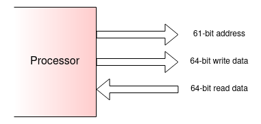
A simple view of a 64-bit processor bus might look something like this:
Here the address bus is 61 bits wide because the lowest 3 bits
address the bytes (only) and there are
23 = 8 bytes across the data buses.
There will also be some control signals: there needs to be an
indication of the direction of a given transaction (write/store
or read/load) and something to indicate if the bus is active or not.
To facilitate write operations of different sizes there needs to be
some indication of the transfer size so that the memory system
does not modify bytes it should not.
(In a real bus there may be other control signals too, but they don't matter too much here. Some examples are mentioned later.)
Imagine trying to fill the memory space with memories which are bought
in 8 GiB units (arbitrary example size) - i.e. 1 GiW at a
time. 30 address bits are needed to select a location within a
unit. This leaves 31 address bits to consider which is space for
about two billion such units.
Some of these other bits are decoded to distinguish RAM from
I/O etc. and some will be wanted to select one RAM or another.
However it is unlikely that all of these need be used.
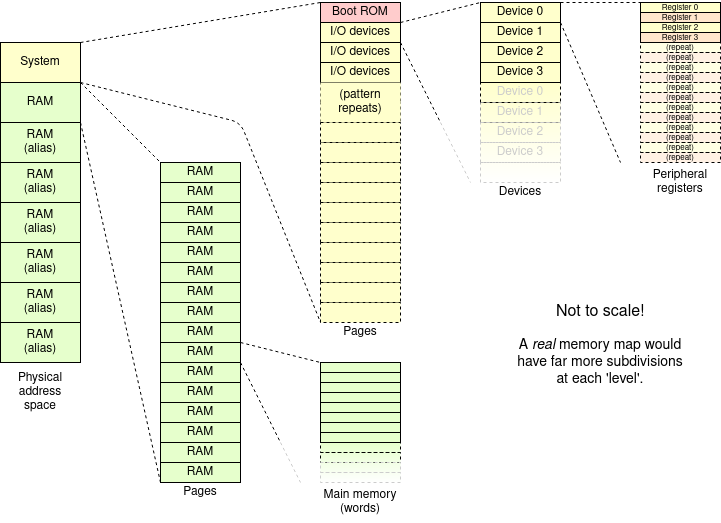
The usual expedient is to ignore some address bits. This means their values don't matter and the (visible) effect is to cause a memory (or I/O) location to appear at repeated positions in the (physical) address space. There may also be (notionally) ‘empty’ areas or spaces ‘for future expansion’ designated.
Here are a couple of address map illustrations from the Web.
(Click image for article/attribution.)
Thus the read latency is the time from wanting some data (from a determined address) and receiving that data.
For a given transaction there is not much that can be done to
reduce read latency although, architecturally there are
mechanisms such as cacheing.
Write latency can be alleviated by write buffering.
Bandwidth can be improved by cycling the bus faster - which may be
difficult in practice - or making the bus wider. The latter approach
is useful when it is known (or expected) that coherent blocks
of data such as cache lines
are being moved; it does not help
with individual ‘random’ transfers.
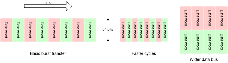
Making buses wider is usually realisable. Note that it increases the number of parallel wires significantly and this can become a problem for pinout if it crosses a chip boundary.
On the other hand, sometimes it is desirable to have a ‘thinner’ data bus, usually in systems (or parts of systems) where speed doesn't matter as much as saving wires: typically I/O functions coming off a chip. In these instances it is normal to have hardware sequencing multiple cycles so the operation is ‘transparent’ to the user.
It is common for systems to support different bus implementations to carry different parts of the address space. There may be a fast, wide bus connection to the RAM, etc. and a slower (simpler, easier to engineer) bus connecting devices which demand less bandwidth, particularly I/O devices. One bus implementation can be converted into another by what is usually called a bus bridge, hence the various terminology Northbridge, Southbridge, Sandy Bridge, Ivy Bridge etc. The field is mired in marketing jargon!
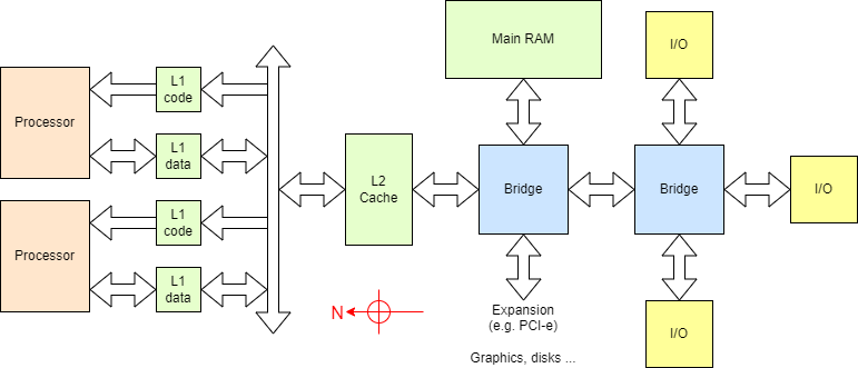
Explore further. There are plenty of examples of system diagrams on the Web, although many are not wholly clear. Here is an example System on Chip (SoC) which has some clear figures: see around p.17.
(There is another example address map on p.54.)Referring to these figures, several features referred to here are visible.
A ‘crossbar’ is a switch which can make any set of non-conflicting connections in parallel. In this case it will allow any master access to any slave.
- Harvard architecture inside the processor: {“DCache” & “ICache”}.
- Multiple buses with bridges.
- Lower frequency operation further from the processor.
- Bus bridged off chip (“External Bus Interface”).
- Bus crossbar switch (“Matrix”).
The implementation of the bus is not really of concern here.
On-chip, and often on PCB where it is feasible it is normal to
use parallel buses with many wires. For more distant
expansion, serial buses (same information but sequenced in
time) is currently preferred: a familiar example might
be PCI
Express.
Another familiar ‘bus’,
USB, doesn't carry
processor signals: it is for peripheral I/O. It's also more
network-like than a traditional bus.
Interfaces with the ‘outside world’ come in many forms. They are mediated by by ‘peripherals’ - specialised devices which translate software operations into the appropriate sequences of signals.
Typically, peripherals will have a number of specialised registers which are used to monitor and control external quantities. For example, if controlling a motor there could be a register which is written to to set the desired speed, and another where the actual speed could be monitored.
Most often these registers are memory mapped i.e. they have unique addresses in the overall address space. Most I/O peripherals only have a small number of associated registers (maybe only one, typically less than 32) so they only require a small part of the address space. They are therefore often placed ‘together’ in the address space. For economy, many address lines may be ignored so various registers/areas will appear as aliased repetitions at regular intervals.
In a simple computer system the memory is only written and read by a single processor. This means it cannot change unexpectedly (at least if the system is programmed correctly!). Once multiprocessors are introduced - including DMA, GPUs etc. memory locations may be changed whilst the processor is ‘not looking’.
I/O - especially the ‘Input’ bit - is expected to change
autonomously. The first significant issue here is to ensure areas of
address space containing peripherals are not cached.
There may be other issues to note, such as changing one register may
cause changes in others.
This gets a bit detailed to delve into here though.
Aside: some processors have additional I/O address spaces, logically separate from the memory space. The most notable example may be the x86 architecture where it is retained for legacy reasons. Here it is a 64 KiB space accessible by the
in andout instructions (analogous to ‘load’ and ‘store’) It is redundant in modern systems.There may be other (usually small) spaces. For example, ARM uses a coprocessor space for some control registers (such as the MMU) which can then be outside the memory mapped space.
Next: bus structures.